Slide 9 of 46
Notes:
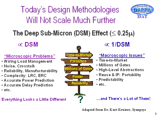
At minimum mask dimensions below 0.25 micron, significant changes begin to appear in the relative importance of parasitic effects in silicon designs, especially interconnect resistance, capacitance, and inductance. These effects, coupled with the complexities and circuit densities possible in such technologies, result in a very different set of tradeoffs in circuit design, architecture, and design verification and test than are appropriate for older technology generations.
Local statistical variations in devices begin to play an important part in long-term reliability and performance and interconnect effects are likely dominate overall system characteristics at 0.18 micron and below. Low power supply voltages and increased signal coupling make the design of high-performance analog and mixed-signal system very challenging.
Chip complexity drives another set of issues. The use of large teams of designers with diverse expertise--possibly 1000’s per design--challenge our abilities in collaborative design and visualization. Design productivity demands design reuse while complex parasitic effects in signals, clocks, and supplies makes such reuse very difficult
There are many challenging research issues in each of these areas, as are outlined in more detail later.