1. Prelab
In this lab we use the microcontroller to synthesize sound and use phasors to manipulate it. Yup, despite the complex(ity), phasors can be very real & even audible!
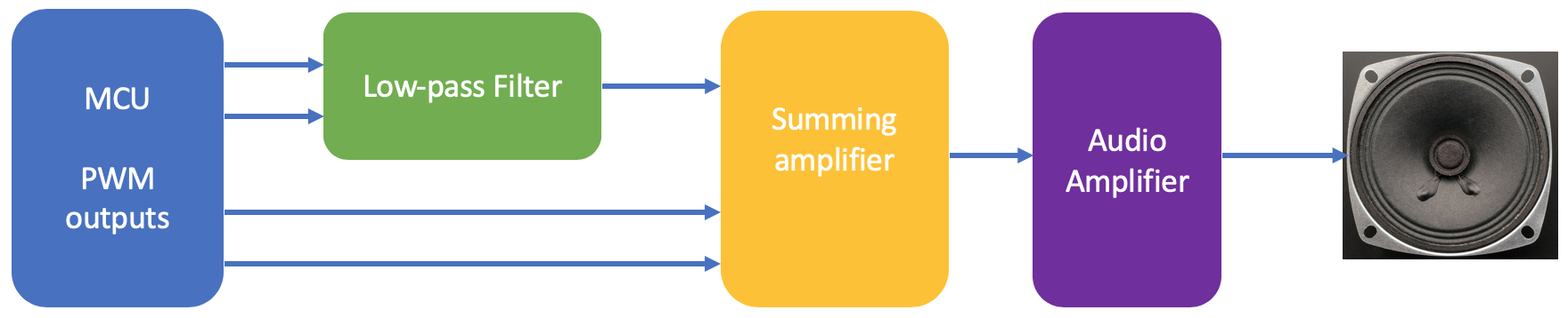
Figure 1 shows a block diagram of the synthesizer. The microcontroller (MCU) generates the audio waveforms, either analog (if your microcontroller has a DAC) or digital (PWM) signals. Two of these are passed through a low-pass filter (LPF) and two go straight to a summing amplifier. The analog filter removes undesired spectral components e.g. from the PWM signals. The resulting signal is gained up for output with a speaker.
Because there are so many parts, let’s design each block separately.
1.1. Filter
PWM square-waves are easy to generate but do not “sound” very good (as you will be able to judge with your own ears in this lab). A filter can fix this: Fourier analysis tells us that all waveforms can be represented as a sum of sinusoids. In other words, a PWM square-wave at frequency fo is just a sinusoid at the fundamental fo plus additional sinusoids at frequencies that are multiples of fo. If we pass a square-wave though a filter that removes all frequencies except the fundamental fo, out comes a sinusoid!
The “removes all frequencies except” part in the previous paragraph is a bit challenging to achieve in practice, but a second-order RC low-pass filter (LPF) does a reasonable job. While doing the design is optional, read at least through the explanations and then answer the following questions:
Gain vo/vi at f = 100 Hz Hint: it’s not 1! |
|
Gain vo/vi at f = 10 kHz |
At the heart of the filter is an operational amplifier. As usual, the power supply is not shown in the circuit diagram, but it surely is required in the actual circuit. To make our project self-contained, we power the opamp, an industry standard LM358A, from the 3.3V supply of the microcontroller breakout board, i.e. the positive supply terminal of the amplifier is connected to 3.3V and the negative to 0V.
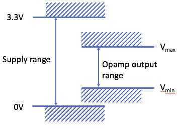
The available output voltage swing of the amplifier is less than the supply, as illustrated in Figure 2. Consult the datasheet to determine the values of Vmin and Vmax. Use the “worst-case” (max) numbers for maximum output current.
Vmin |
|
Vmax |
The available range is quite a bit smaller than the supply voltage range. This can be a problem, especially in applications with low supply voltages. So-called “rail-to-rail” operational amplifiers can produce output voltages that are very close to either supply rail. As an example, look up the typical values of Vmin and Vmax for the LT1997-2 with 3.3V supply for no load and 5mA output current.
Vmin |
|
Vmax |
Unfortunately most of these more modern and “better” amplifiers are not available in breadboard friendly dual in-line packages and therefore not easy to solder.
To deal with the reduced swing, we need to slightly modify the filter circuit by connecting the positive input of the opamp to an appropriate voltage Vmid. Let’s assume that we were using an operational amplifier whose output could swing from 1.2V to 1.8V. The input vi is a square wave changing between 0V and 3.3V.
Find the values of Vmid and R1 at low frequency (DC) for R2 = 10 kΩ.
Vmid |
|
R1 |
Show your analysis in the space below:
Verify that the output vo stays within the available swing.
| vi | vo |
|---|---|
0 V |
|
3.3V |
1.2. Summing Amplifier
To investigate (and listen to) the effect of the filter, we want to send both filtered and un-filtered PWM waveforms to the speaker. To accomplish this, we synthesize several signals with the MCU and sum the different versions with a second opamp, as illustrated in Figure 1.
Design a summing circuit with three inputs using an opamp with equal gains such that the output is 5V when all inputs are 0V and 0V when all inputs are 5V. While your solution will probably resemble an inverting amplifier configuration, extra components will be needed to determine the output into the proper range.
Show your circuit and analysis below. Mark all components and their values in the schematic. In the lab we will be using different component values specified in Table 1 that meet all these constraints.
Note that this is a simplified version of the actual design problem which requires all voltages to remain within the limits of the amplifier input and output ranges calculated in the previous section. Also, a higher supply voltage than 3.3V would be needed for this circuit to work.
1.3. Audio Amplifier
The output power from the operational amplifier is too low to drive a speaker. The PAM8302A class D audio amplifier delivers up to 2.5W.
The PAM8302A breakout board contains a few additional components. Figure 3 shows the schematic diagram. The differential input AIN+, AIN- is applied to the amplifier through a potentiometer (for manual volume adjust) and capacitors C1 and C2. The latter provide “ac coupling”: the bias voltage of the amplifier is set (internally to the amplifier) independent of the bias (mid-point) of AIN+, AIN-. Very low frequency components are filtered out since AC coupling effectively acts as a high-pass filter. Since audio signals are above approximately 20Hz, this is no problem.
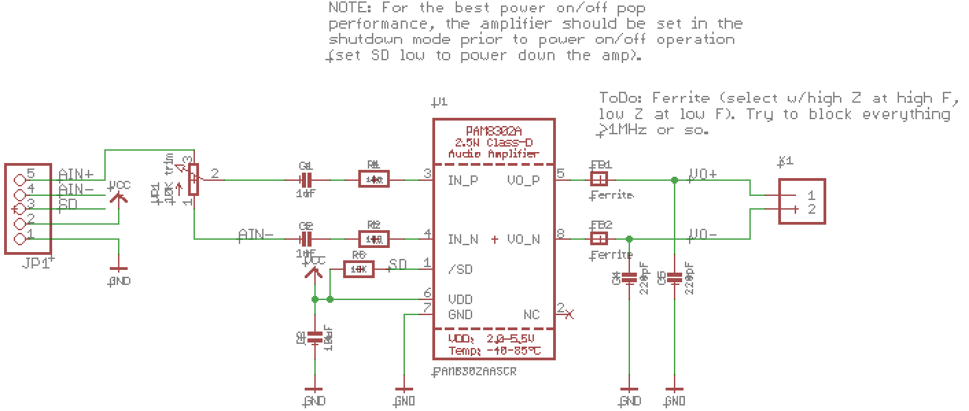
AC-coupling is convenient and used frequently. However, there is one inconvenience that we need to take care of: upon power-up the capacitors are discharged. Since the output from opamp OP2 AIN+ quickly rises to about 2.5V (AIN- is connected to ground), a DC voltage momentarily appears across the speaker (VO+, VO-), resulting in an audible “pop”. As capacitors gradually charge, the DC decays to zero.
|
What is a “class D” amplifier? Just like modulating the brightness of an LED, varying the power delivered by an amplifier can be accomplished by rapidly turning the output on and off (typically at about 200kHz for audio amplifiers). Compared to linear amplifiers (e.g. opamps) this solution is much more power efficient. In addition to the power savings, it also alleviates the need for cooling fins attached to the amplifier. Class D amplifiers are used in all applications that require low power dissipation and cost, such as smart phones. The extra circuit complexity is absorbed in the amplifier IC at negligible added expense. The high-frequency “distortion” is removed by the low-pass characteristic of the mechanical elements in the speaker, the ferrite beads |
1.4. Printed Circuit Board
Rather than the solderless prototyping boards used in other labs, we use custom Printed Circuit Board (PCB) for this lab. PCBs are the standard technology used to wire electronic components. Unfortunately we do not have the time in the lab to design our own, but all the tools to do so, along with many tutorials, are available for free online. Feel free to explore!
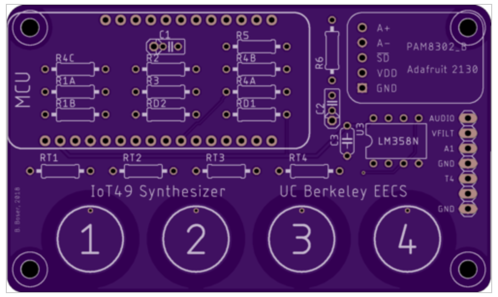
Figure 4 shows the complete schematic used in this lab. Figure 5 shows the PCB. It has been designed with Eagle CAD. The design files for the schematic and board layout are available for download to experiment with.
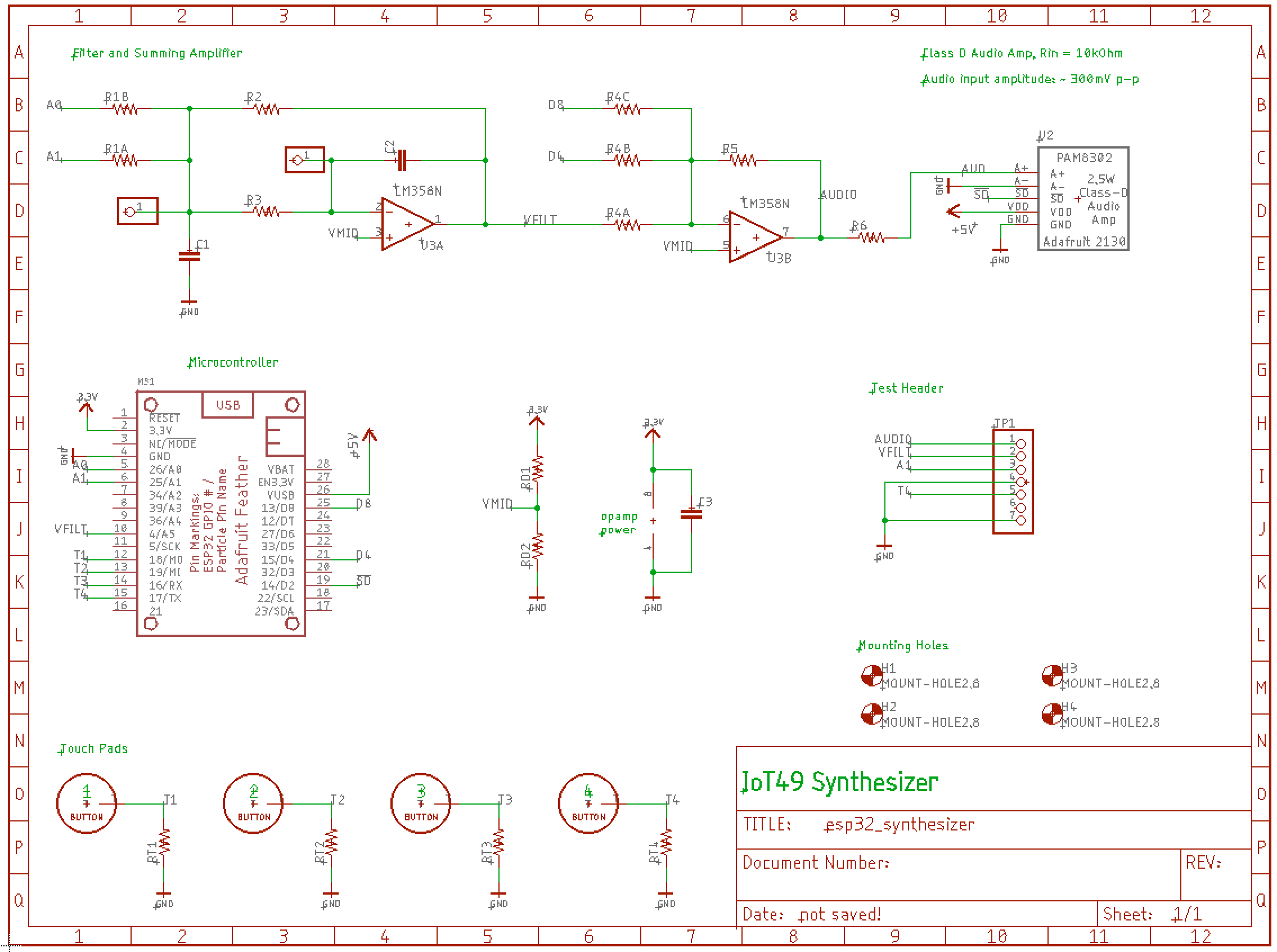
WATCH OUT! The pin naming in the schematic symbol for the ESP32 (“Adafruit Feather”) shows the wrong names. Instead of the name use the number shown next to each pin (the one inside the rectangle) in your code when referring to pins! E.g. to refer to the pin connected to node A0 use code similar to Pin(26, …). For node D4 the code is Pin(15, …).
|
1.5. Firmware
The synthesizer software, filling in the skeleton below:
# imports ...

# initialize PWM objects for all synthesizer inputs

pwm_filtered = ...    # PWM waveform A0 that passes through the filter
pwm_1 = ...           # PWM waveform D4 passed to amplifier without filtering

def play(pwmout, enable=False, freq=freq):
    '''if enable, generate pwm signal on pwmout with specified frequency
       otherwise set the pwm output to 0.'''
    # Hint: adjust the duty cycle to achieve this functionality
    # ...

# enable the amplifier ...

# alternatively play the filtered and unfiltered output
freq = 1000
filtered = True
while True:
    play(pwm_filtered, enable=filtered, freq=freq)
    play(pwm_1, enable=not filtered, freq=freq)
    print("playing, filtered", filtered)
    sleep(2)
    filtered = not filtered
Save and submit your code as synthesizer.py. Have it ready in the lab for testing!
1.6. Oscilloscope
Familiarize yourself with the oscilloscope by reading the instructions in part B of the document.
2. Lab
2.1. Soldering
First, solder the PCB components. Use the following values:
| Component | Value | Component | Value |
|---|---|---|---|
R1A |
150 kΩ |
R1B |
optional |
R2 |
22 kΩ |
R3 |
47 kΩ |
R4A |
22 kΩ |
R4B |
150 kΩ |
R4C |
390 kΩ |
R5 |
10 kΩ |
R6 |
6.8 kΩ |
RD1 |
1.8 kΩ |
RD2 |
1.2 kΩ |
RT1 … RT4 |
10 MΩ |
C1 |
10 nF |
C2 |
2.2 nF |

Many ways to solder the board. Usually it’s better to start with small components (e.g. resistors) and add tall components last. Use pliers or a wire bender tool (Figure 6) to bend leads. Note that two via options are provided for capacitors of different size. Choose the one that fits best (place the component over the capacitor symbol!).
Be careful when soldering components with several pins, such as amplifiers and headers. Solder a single connection first and check if the component is seated correctly, making adjustments as needed. Then solder the other pins.
Watch out for cold solder joints, and beware that metal is a good conductor: do not touch any metal surface (e.g. a header) while soldering.
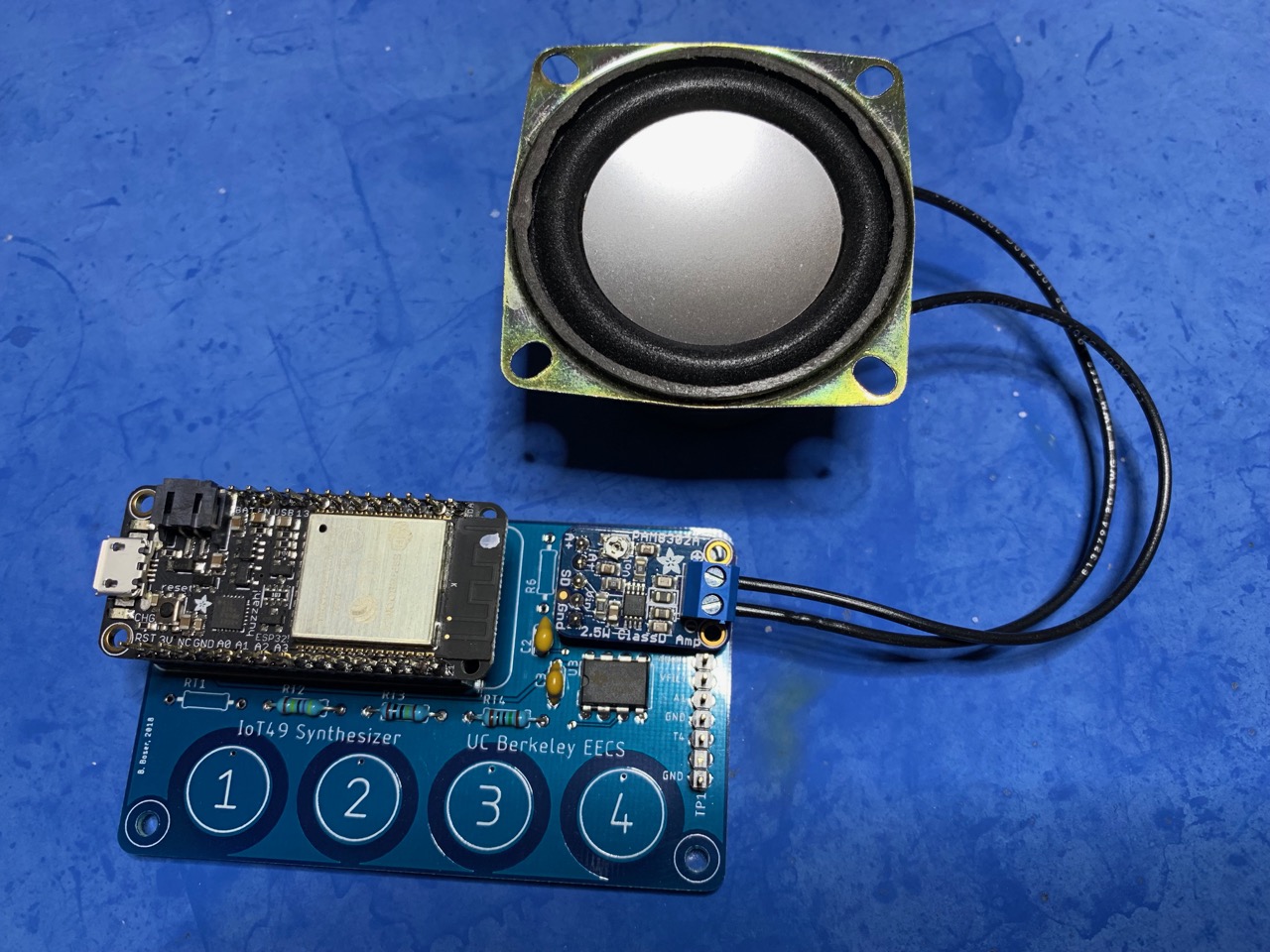
Figure 7 shows the partially assembled board.
| Proceed carefully; replacing soldered components is difficult and carries the risk of damaging the printed circuit board. |
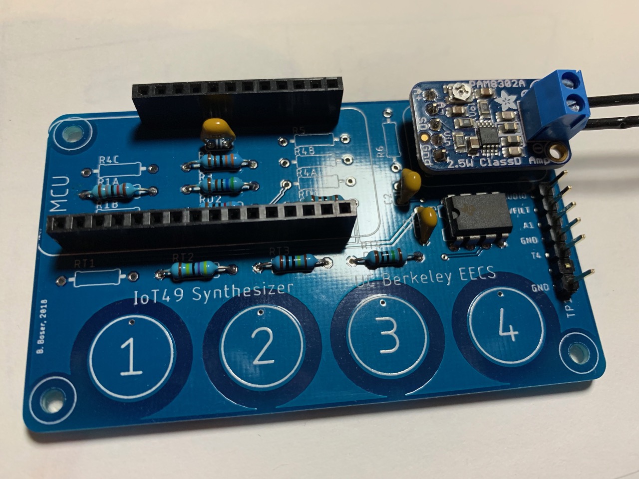
Show your soldered board to the instructor . Only after the checkoff insert the microcontroller.
2.2. Synthesizer
Connect the oscilloscope to connections A1 and VFILT on the test header. Then run the code to generate a square wave on pin A1. Start with 100Hz and observe the filtered output. It should be looking very close to a square wave. Gradually increase the frequency and observe the change of the output. Explain the shape of the waveform at 500Hz. At what frequency does the output start looking like a sinusoid?
Show the input and output waveforms at 500Hz and 1500Hz to the instructor.
2.3. Sound!
Now it’s time to compare the sound from filtered and un-filtered square waves. Enable the speaker and play each waveform for a few seconds before switching to the other. Can you tell them apart? Which do you prefer?
The ear is very sensitive to volume. To help differentiating between the effect of the filter and different volumes, output D8 has lower gain than D4. Try comparing A1 to D8 to make the volumes of the two waveforms more equal. Does your preference change?
Demonstrate your achievement to the instructor!
2.4. Optional
The synthesizer is quite flexible and can produce a large range of sounds, including polyphonic music. Experiment!
It is also possible to play tunes[1]:
# define frequency for each tone
C3  = 131
CS3 = 139
D3  = 147
DS3 = 156
E3  = 165
F3  = 175
FS3 = 185
G3  = 196
GS3 = 208
A3  = 220
AS3 = 233
B3  = 247
C4  = 262
CS4 = 277
D4  = 294
DS4 = 311
E4  = 330
F4  = 349
FS4 = 370
G4  = 392
GS4 = 415
A4  = 440
AS4 = 466
B4  = 494
C5  = 523
CS5 = 554
D5  = 587
DS5 = 622
E5  = 659
F5  = 698
FS5 = 740
G5  = 784
GS5 = 831
A5  = 880
AS5 = 932
B5  = 988
C6  = 1047
CS6 = 1109
D6  = 1175
DS6 = 1245
E6  = 1319
F6  = 1397
FS6 = 1480
G6  = 1568
GS6 = 1661
A6  = 1760
AS6 = 1865
B6  = 1976
C7  = 2093
CS7 = 2217
D7  = 2349
DS7 = 2489
E7  = 2637
F7  = 2794
FS7 = 2960
G7  = 3136
GS7 = 3322
A7  = 3520
AS7 = 3729
B7  = 3951
C8  = 4186
CS8 = 4435
D8  = 4699
DS8 = 4978

# scale
scale = [
    C4, CS4, D4, DS4, E4, F4, FS4, G4, GS4, A4, AS4,
    B4, C5, CS5, D5, DS5, E5, F5, FS5, G5, GS5, A5, AS5, B5, C6, CS6, D6,
    DS6, E6, F6, FS6, G6, GS6, A6, AS6, B6, C7, CS7, D7, DS7, E7, F7, FS7,
    G7, GS7, A7, AS7, B7, C8, CS8, D8, DS8]

# Mario Bros
# http://www.linuxcircle.com/2013/03/31/playing-mario-bros-tune-with-arduino-and-piezo-buzzer/
mario = [
    E7, E7, 0, E7, 0, C7, E7, 0, G7, 0, 0, 0, G6, 0, 0, 0, C7, 0, 0, G6,
    0, 0, E6, 0, 0, A6, 0, B6, 0, AS6, A6, 0, G6, E7, 0, G7, A7, 0, F7,
    G7, 0, E7, 0,C7, D7, B6, 0, 0, C7, 0, 0, G6, 0, 0, E6, 0, 0, A6, 0,
    B6, 0, AS6, A6, 0, G6, E7, 0, G7, A7, 0, F7, G7, 0, E7, 0,C7, D7,
    B6, 0, 0]

# play Bach Prelude in C.
bach = [
    C4, E4, G4, C5, E5, G4, C5, E5, C4, E4, G4, C5, E5, G4, C5, E5,
    C4, D4, G4, D5, F5, G4, D5, F5, C4, D4, G4, D5, F5, G4, D5, F5,
    B3, D4, G4, D5, F5, G4, D5, F5, B3, D4, G4, D5, F5, G4, D5, F5,
    C4, E4, G4, C5, E5, G4, C5, E5, C4, E4, G4, C5, E5, G4, C5, E5,
    C4, E4, A4, E5, A5, A4, E5, A4, C4, E4, A4, E5, A5, A4, E5, A4,
    C4, D4, FS4, A4, D5, FS4, A4, D5, C4, D4, FS4, A4, D5, FS4, A4, D5,
    B3, D4, G4, D5, G5, G4, D5, G5, B3, D4, G4, D5, G5, G4, D5, G5,
    B3, C4, E4, G4, C5, E4, G4, C5, B3, C4, E4, G4, C5, E4, G4, C5,
    B3, C4, E4, G4, C5, E4, G4, C5, B3, C4, E4, G4, C5, E4, G4, C5,
    A3, C4, E4, G4, C5, E4, G4, C5, A3, C4, E4, G4, C5, E4, G4, C5,
    D3, A3, D4, FS4, C5, D4, FS4, C5, D3, A3, D4, FS4, C5, D4, FS4, C5,
    G3, B3, D4, G4, B4, D4, G4, B4, G3, B3, D4, G4, B4, D4, G4, B4
]

# initialize PWM output
synthesizer = ...

def play(tune, t=300):
    for f in tune:
        if f == 0:
            # turn of sound (e.g. set duty cycle to 0)
            # ...
        else:
            # set frequency and 50% duty cycle
            # ...
        sleep_ms(t)
    # turn off sound
    # ...
    sleep(1000)

play(scale, 100)
play(bach,  200)
play(mario, 150)