We have constructed a large SPACE system as part of the PADMAVATI project [Guichard-Jary1990]. Full custom VLSI SPACE chips are packaged using Tape Automated Bonding onto compact SPACE modules. These modules are attached to conventional circuit boards, which are then connected by a backplane to host processor boards within a MIMD parallel computer system. The following sections describe each level in the packaging hierarchy.
The SPACE chip implements a small version of the SPACE programming model described in Figure 1. Each chip contains an array of 5328 static CAPP cells arranged as 148 words of 36 bits, a 148-bit flag chain, 36-bit Mask and Write-Enable registers and a 148-input priority resolution tree. The array is never coordinate addressed, so there is no incentive to make the number of words per die a power of two. A conservative 16 transistor static CAPP cell design was adopted to simplify design and ensure robustness. Priority resolution was implemented using a high-radix tree to reduce the latency of selection operations.
The SPACE chip has 56 pins: 7 instruction inputs, a 36b tri-state data bus, 4 pins for cascading chips (pins PRF , NXF , REQ and PRQ ), 3 timing and control inputs (pins CS , CE and PCH ), and 6 power supply connections.
PRF and NXF are tri-state pins used to connect the flag chain of a chip to the previous and next chips' flag chains respectively. REQ and PRQ are used to connect the internal priority resolution tree as a leaf node of an external priority resolution tree. A chip asserts REQ if it contains selected words, the external tree asserts PRQ if any preceding chip asserted REQ . Each SPACE chip in a large system maintains its own copy of the Mask and Write-Enable registers. For write register operations all registers are updated in parallel. For read register operations, the priority resolution tree is used to ensure that only the first chip in the array responds with the values stored in these registers.
The CS input is used to partition a large array into independent banks. When low, it disables all chip operations and outputs. Multiple selected chips must be adjacent if flag chain continuity is to be preserved. This feature was added to allow a large SPACE array to be partitioned amongst a number of different applications. For example, on the PADMAVATI machine the run-time system may use one bank to speed global address translation for interprocess communication while the rest of the array is made available for user applications.
SPACE chip timing is controlled by the CE input. The PCH
pin controls the internal prechargers. It can be tied high in which case the chip is fully static but burns more power, or can be pulsed high between supplying the data and strobing CE .
The SPACE chips were fabricated in a 1.2  m two-level-metal n-well
CMOS technology from a fully-custom layout. The die measures
5.8
m two-level-metal n-well
CMOS technology from a fully-custom layout. The die measures
5.8 7.9mm
7.9mm and contains over 80,000 transistors. The minimum
chip cycle time is 125ns.
and contains over 80,000 transistors. The minimum
chip cycle time is 125ns.
Figure 2 is a photomicrograph of the chip. Samples were received in June 1989 and passed all functional and speed tests first time, thanks to extensive functional and electrical simulation prior to fabrication. Over 1,200 working parts have since been fabricated for the PADMAVATI project. A more comprehensive data sheet is available [Howe and Asanovic1990].
Figure 2: SPACE Chip.
A SPACE module contains twelve SPACE chips, buffering and one stage of external priority resolution, and is functionally equivalent to a 1776-word SPACE chip. There are numerous advantages to mounting the chips on modules rather than directly onto a large circuit board. Fabrication, testing and repair are simplified, and the modules can be reused in different target systems.
Each module measures 100 60mm
60mm and holds twelve 56-pin SPACE
chips plus seven 20--28 pin SSI/MSI components. Tape Automated Bonding
(TAB) is used to bond the SPACE chips to the module PCB; the remaining
components are surface mounted. With TAB, each SPACE chip has a PCB
footprint of only 12
and holds twelve 56-pin SPACE
chips plus seven 20--28 pin SSI/MSI components. Tape Automated Bonding
(TAB) is used to bond the SPACE chips to the module PCB; the remaining
components are surface mounted. With TAB, each SPACE chip has a PCB
footprint of only 12 10mm
10mm . The module PCB has power and ground
planes, and 4 signal layers with a trace pitch of 0.5mm
. The
pin-out of the SPACE chip was designed to allow devices to be tightly
tessellated on the module PCB. Each face of the die has the
connections for one data byte. Since all four data bytes within a word
are equivalent, the north facing data byte of one die can be directly
connected to the south facing data byte of another die, minimising the
area needed for routing and vias on the module PCB.
. The module PCB has power and ground
planes, and 4 signal layers with a trace pitch of 0.5mm
. The
pin-out of the SPACE chip was designed to allow devices to be tightly
tessellated on the module PCB. Each face of the die has the
connections for one data byte. Since all four data bytes within a word
are equivalent, the north facing data byte of one die can be directly
connected to the south facing data byte of another die, minimising the
area needed for routing and vias on the module PCB.
Each PADMAVATI processor node occupies a standard 280 233mm
233mm 6u
board and includes a 25MHz Inmos T800 transputer with 16MB of 200ns
DRAM and a 32b asynchronous bus interface. SPACE boards have the same
form factor and connect to the processor through the bus interface.
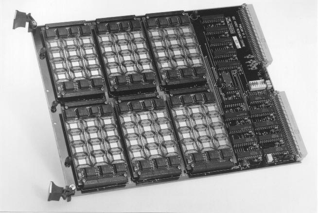
Figure 3 is a photograph of a SPACE board. Each
board holds six SPACE modules, and each operation can select any
subset of the six modules. The selected subset then acts like a single
SPACE chip with up to 10656 words.
6u
board and includes a 25MHz Inmos T800 transputer with 16MB of 200ns
DRAM and a 32b asynchronous bus interface. SPACE boards have the same
form factor and connect to the processor through the bus interface.
Figure 3 is a photograph of a SPACE board. Each
board holds six SPACE modules, and each operation can select any
subset of the six modules. The selected subset then acts like a single
SPACE chip with up to 10656 words.
Figure 3: SPACE Board.
The transputer acts as the microcode sequencer for the SPACE array, sending instructions and data over the inter-board bus. The SPACE array is memory mapped, with instructions encoded on the bus address lines. SPACE board write and search operations are pipelined, and have a minimum cycle time of 320ns. SPACE read operations require a wait for the returned value, and have a minimum cycle time of 480ns. The transputer limits the rate at which instructions are issued to the board. Measurements on the PADMAVATI prototype give an average instruction cycle time of around 1250ns. A more tightly coupled, dedicated microcontroller could reduce the board cycle time for each SPACE instruction to around 160ns with the existing modules.
The final level of packaging yields a complete PADMAVATI system.
Sixteen transputer/SPACE nodes are fully connected through a custom
VLSI dynamic routing switch that obeys the transputer link protocol
[Rabet et al.
1990]. By partitioning the SPACE array amongst the transputers
in this manner, we gain higher array I/O bandwidth and the flexibility
of MIMD control of SIMD subarrays. The total associative storage
capacity is 170496 36b
words, or around 750KBytes. The complete
system is attached as a compute server to a host Sun workstation.
36b
words, or around 750KBytes. The complete
system is attached as a compute server to a host Sun workstation.