Guest Lecturer: Mike Deering
(michael.deering@eng.sun.com)
3D RAM based frame buffer can sustain an overall 10X improvment over traditional designs.
|
|
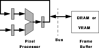
Figure 1 shows the how a traditional system with Z-buffering and RGB blending does a read-modify-write. The pixel processor, typically the main CPU repeats the following:
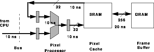 |
Figure 2 shows the 3DRAM write-only interface. The chip presents and interface where writes encode commands to the chip. The ALU read-modify write cycle now happens inside the chip; thus a much higher rate of operations can be sustained. The chip can support 100 million pixels per second.
All ALU operations are pipelined; the cycle time is 10 ns. The ALU is 9 bits wide, 7 and stages? deep. It supports a variety of operations including mulitply-adds, comparisons, and bit operations. The ALU can sustain two 32 bit reads (one from the processor, the other from the cache) and a write per cycle.
The logic for the chip is implemented in a .55 micron process and uses only 1 layer of metal. Mike "guessed" that logic would be 2x-3x slower in a DRAM process than a logic process of the same time-frame. He noted that there is a lack of experience, tools, and libraries for doing logic in DRAM. Dave P. noted that back in the "the old days" (when most of us we just figuring out space-invaders) real designers built processors from transistors. In a later class John W. noted that in "the old days" processors where built from a single layer of metal too.
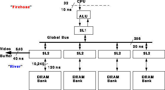 |
Figure 3 shows the on-chip memory hierarchy. The hierarchy is needed to solve the "speed mismatch" or "impedance" problem. Mike used the following analogy: The top of the memory is like a fire-hose; a small about of water(bits) is moving at 100 miles/hour. The bottom is like a mile wide river moving at 1 mile/hour. Clearly, the river can move more water (bandwidth). However, we care not only about the amount of water but also is absolute speed. The design challenge is to enable a small amount of fast moving water using a huge amount of slower water.
The L1 cache is diveded into 8 256-bit blocks. It is a write-back cache with N-way associativity. Figure 2 shows that the L1 cache is triple-ported. It supports 32 bit read and write port to the ALU, and a 20 ns 256-bit port to the global bus . An interesting aspect of the cache is that the cache-control logic is off-chip. More on this design choice will be covered in the next section.
The global bus is a 256-bit wide bus connecting the L1 and L2 caches. The bidirectional bus can move 256 bits (the L1 block size) every 20 ns.
Each of the 4 L2 caches corresponds to the sense amps on one DRAM block. The L2 cache is 10,240 bits wide and has three ports: one 256-bit wide port to the global bus, a 640 bit-wide port to the video buffer, and a giant 10,240 bit port to the DRAM. Because it corresponds so nicely to the DRAM block, it is direct mapped and write-though. Every 600 ns an L2 cache must give up a block to the video output.
The key point of this heirarchy is that it takes advantage of the spacial locality of graphics operations. Both the L1 and L2 are organized into rectangular blocks, instead of the traditional "long skinny" blocks in page-mode VRAM, for example. The memory hierarchy spreads out the narrow "fire hose" into a slower moving "river".
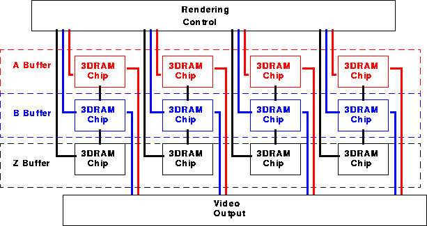 |
Figure 4 shows a 1280x1024 double and Z-buffered frame buffer. This design is constructed using 12 3DRAM chips, a rendering/control chip and a video output chip.
Figure 4 shows how the 3D RAMs operate as bit-sliced system. The controller chip (ALU and cache control!) reside outside the 3DRAM. Each 3DRAM operates in parallel on a different part of the frame buffer.
	Primitive	Size		Rate

	Tiangle		50 Pixel	2-4M/sec
			100 Pixel	1.5-1.8M/sec

	Vector		10 Pixel	3.5-7.5/sec

	Fast Clear	Block Fill	1.2-1.6G pixels/sec
			Page Fill	24-32G pixels/sec

	Image Copy	Write		264-400M pixels/sec
			Read		132-200M pixels/sec