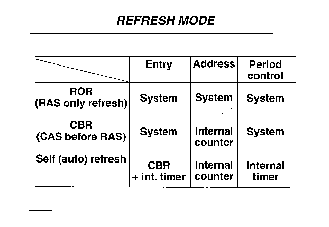
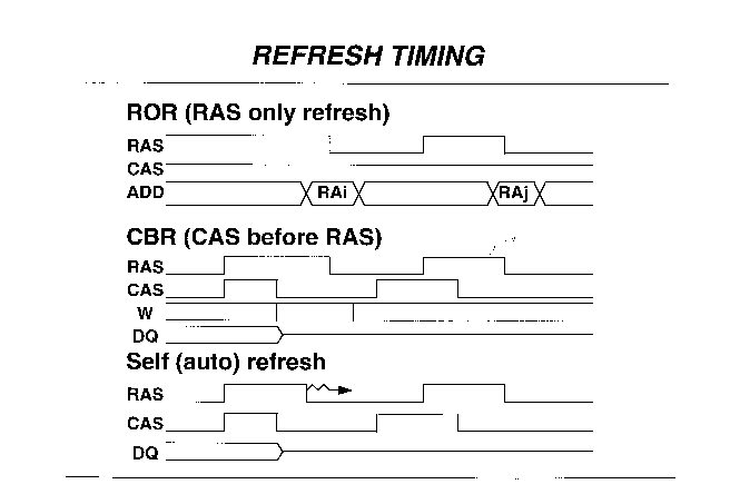
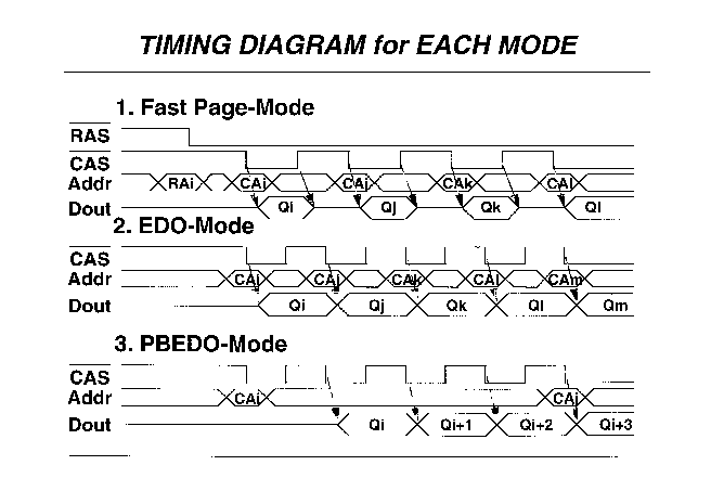
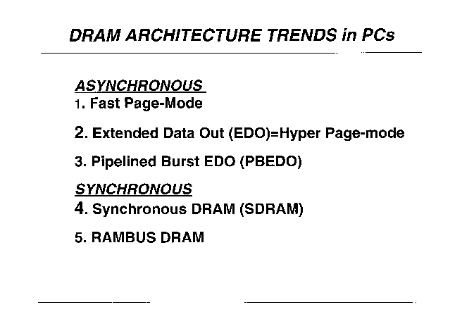
The following is a slide presentation given by Changhyun Kim of Samsung Electronics on Basic Dram Operation. Also included are two slides from his ISSCC presentation on a 1-GB DRAM. A summary of the key points is included throughout the slides.


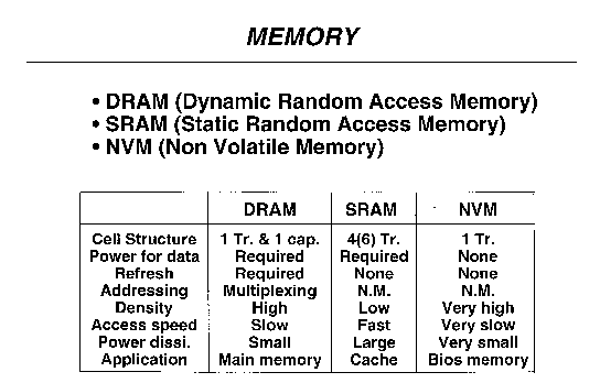
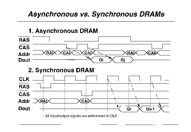
- Multiplexed addressing contributes to the slowness of DRAM.
- Power dissipation in SRAM is large because of faster access.
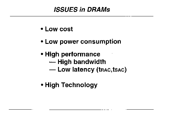
- Typically, the better performance you have, the higher the power requirement.
- The power loss in an SRAM due to leakage current is significant, at 1 nA.


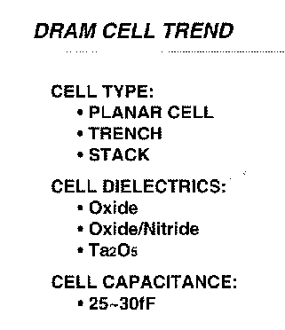
- The cell type used in DRAM is company dependent.
- The 25-30 fF capacitance value is a rule-of-thumb value, valid across all generations.
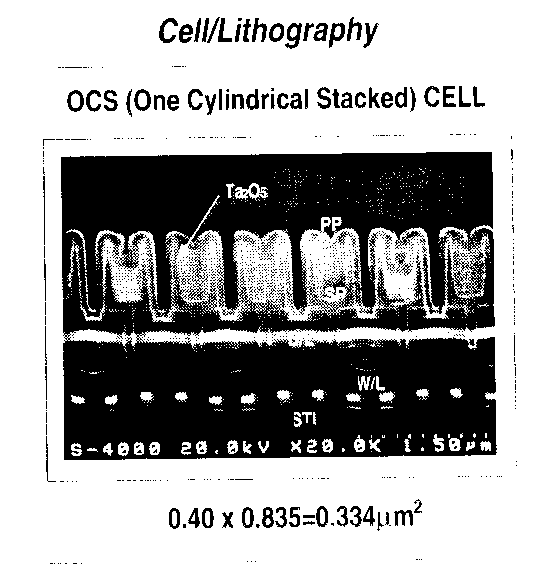
- One can increase the capacitance with a change in the dialectric. (Ta2O5 yields a higher capacitance.)
- A trench cell is good for smaller packaging.
- A trench cell is also susceptible to noise from the substrate.
- Logic consumes a lot of power and injects noise into the substrate, and this could be bad for trenched cells.
- The stacked cells can be affected by noise in the upper layers.
- Stacks are more popular and are easy to make small.
- Stacks are easier for Samsung to build than the trench.
- The stack lends itself well to mass production.


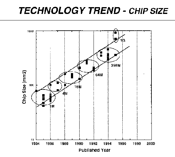
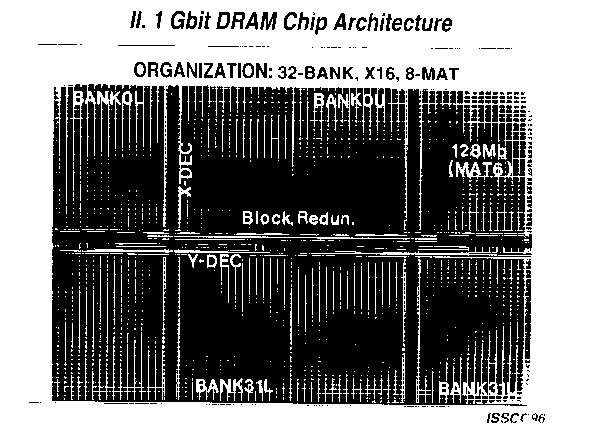
- The new 1 GB chip from Samsung is 652 mm2.

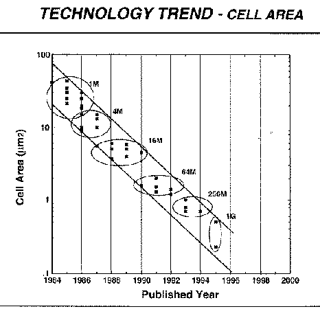
- The new 1 GB chip from Samsung is .2 um2.

- Many DRAMs operate at 5 V off chip, and at 3.3 V for internal chip operation.
- The 1 GB DRAM from Samsung used 1.8 V for the memory array.
- The 16 MB and 64 MB DRAMs use 3.3 V, internal 2.5-2.6 V.
- The location on the bonding pad varies with company.
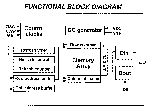
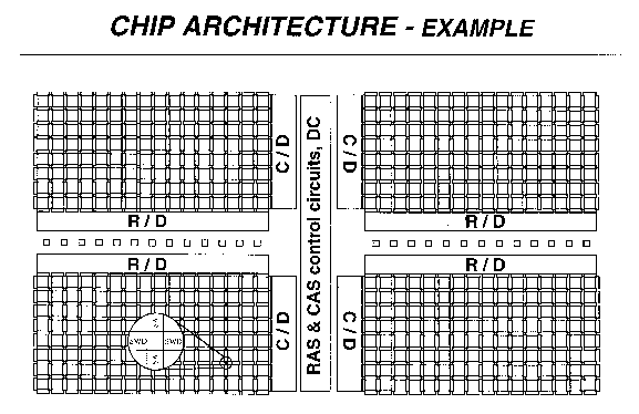
- Data lines run perpendicular to the bit lines. Multiplexing is done at the sense amps, and only a few data lines emerge from a whole row of sense amps.

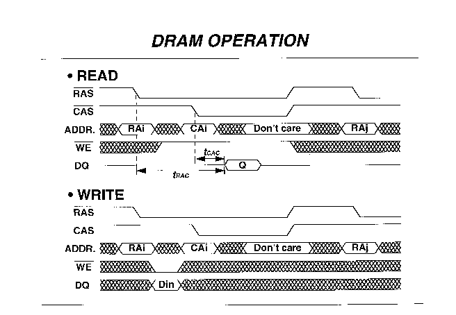
- During write enable, between row and column address, we keep data in a buffer.
- How many I/O lines do we need? This depends on the refresh time and how many I/Os we have.

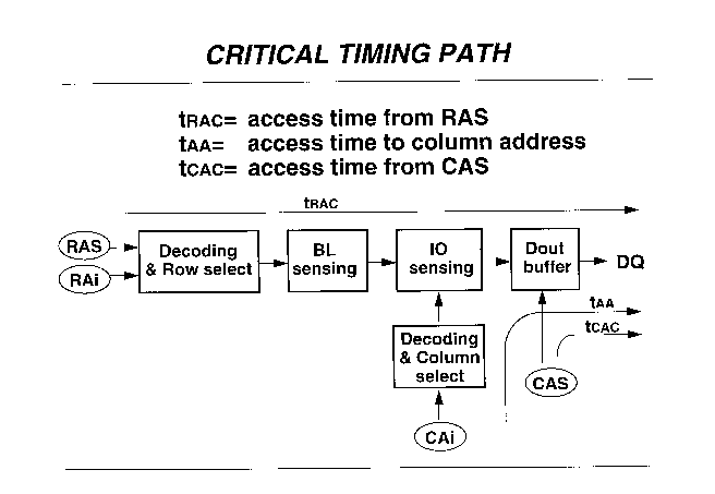
- tRAC : 50-60 ns (worst case), 30-40 ns (best case)
- tAA : 20 ns
- tCAC : 10 ns
- Bit Line sensing takes the most time.
- tRAC for the 1 GB Dram is 31 ns.
- Eliminating driving the data off-chip could eliminate 5ns from critical path.
- These times are technology dependent.
- Slower SRAMs have 20 ns access time, so a fast DRAM could be compatible with a slow SRAM.
- A DRAM without a muxing scheme could have the same performance as an SRAM.
- Packaging size of SRAM to DRAM is 5:1 because of more I/O on the SRAM.

- .5*VCC used for bitline voltage precharge
- The bitlines diverge by ~ 200 mV, depending on the power supply voltage.
- Delta(V_bc) = C_s/(C_b + C_s) where C_b is the bit line capacitance
- It doesn't matter whether you turn on SAN before SAP when alternating bitlines.
- Aluminum is used to run the I/O out. Choose the metel depending on the process.
- It is possible to run more I/O over the data cells.


- EDO Mode => We can reduce CAS cycle time because the Data Out Hold Time is longer.
- EDO => 50 MHz
- PBEDO => Higher clock rate (50-60 MHz)
- FPM => 31 - 33 MHz


- A lot of delay is due to transistor driving capability.

- OCS cell => one cylindrically stacked cell
- OCS cell area is .334 um2.

- The package size for the 1 GB DRAM is 2 cm x 3 cm.
Closing Remarks
- The substrate can be biased in order to get a higher threshold voltage. The 1 GB DRAM is biased to -1 Volts. Others are commonly biased to -2 or -2.5 V.
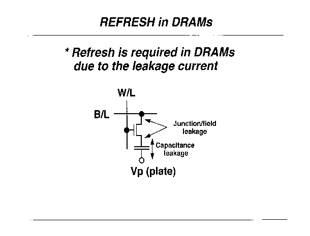
- The dominant leakage problem is increasing substrate leakage with higher densities. Junction leakage depends on the process.
- A current sense amp is slightly faster than a typical voltage sense amp.
- The simplest sense amp is 4 transistors. A current sense amp is 6 transistors.
- For high loading, we use a current sense amp.
- If we double the I/O lines, we get double the bandwidth. There is no need to change the design, but the more I/O lines we have, the greater the noise and power consumption.
- One of the worries in adding logic to a DRAM is power consumption. Logic has a lot of power and makes a lot of noise. DRAM is very susceptible to noise. There is also the issue of process compatibility.
- Embedded logic in DRAM would be good for high performance chips.
- SRAM is more compatible with a logic process.
