EE290A Homework 3 Report
Rhett Davis, Ning Zhang, Chris Tayor, David Chinnery
I. Introduction to InventraTM Viterbi encoder/decoder soft core
-
Features
-
Flexible coding parameters: code rate, constraint length, traceback depth,
code generating functions, soft decision word length
-
Two orders of magnitude flexibility in speed and area: full parallel for
high speed, and parameterized resource sharing for area efficiency
-
Robust algorithmic implementation: self-normalizing traceback and saturation
arithmetic in ACS computation
-
RTL model optimized for high quality synthesis results
-
Additional features (which can be disabled): channel bit error rate monitoring,
Viterbi encoder, and synchronization monitor
-
Deliverables
-
Bit-true cycle-based C and VHDL behavioral models
-
Synthesizable and simulatable VHDL models with simulation scripts for Mentor
VHDL simulator (which did not work for Synopsys VHDL simulator however)
-
Self verifying test bench
-
Synopsys synthesis scripts
-
User's guide
II. Our implementation based on the Mentor Viterbi soft core
-
Parameters
-
code rate = 1/2
-
constraint length (L) = 7
-
code generating functions: g0 = 171, g1 = 133
-
soft decision word length (q) = 6
-
traceback depth (D) = 48
-
accumulated state metric word length (swidth) = 9
-
number of parallel ACS units implemented in hardware = 4
-
Functionality verification and bit error rate (BER) simulations
As part of the Viterbi decoder soft core deliverables, three functionally
equivalent models are provided: a synthesizable VHDL RTL model, a behavioral
bit-true VHDL model, and a bit-true C behavioral model. The equivalency
of the models for the particular decoder parameters of interest was verified
through C and VHDL (modelsim) simulations, while the simulation times for
the three models differ significantly (the behavioral VHDL simulation was
about 10 times slower than behavioral C simulation, and the VHDL RTL
simulation was about 1,000 times slower).
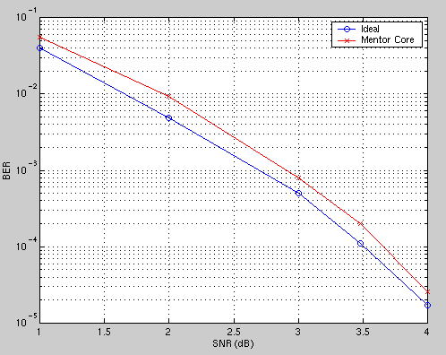
The C behavioral model was used for BER simulations. It is a true cycle
based implementation offering the highest simulation speed. The decoder is
implemented
using integer arithmetic with identical precision and rounding algorithms
as the RTL model. The figure below shows the BER against SNR (signal to noise)
curves for both
"ideal" (D = 100 and floating point or swidth = 11 with modulo arithmetic
in the ACS unit) and Mentor core (D = 48 and swidth = 9 with normalization)
cases. The SNR degradation is about 0.15 dB.
The synthesized net list of the Viterbi decoder is simulated and the
gate level simulation results are compared with those form behavioral
simulation to verify the functionality of the synthesized hardware (i.e.,
no synthesis related errors were introduced and timing constraints are
met under target condition). After place and route, a transistor level
net list with parasitic capacitance can be extracted and final verification
could be done using Epic tools.
-
Technology
-
Technology used was 0.25 um with a good standard cell library from ST Microelectronics,
with six metal layers.
-
Design flow
-
Synthesis
-
Synthesis was performed assuming a cycle time of 15 us (effectively infinite)
-
Performance
-
A speed of 100 ksps was achieved at a clock speed of 1.6 MHz.
-
With the clock speed reduced to 1.6 MHz and supply voltage scaled down
to 0.8 V, the power was 0.14 mW (0.03 mW/mm2).
-
The signal degradation was 0.15 dB with the test data provided.
-
Cost
-
The final chip area was 4.00 mm2.
-
The Inventra Viterbi soft core costs $100,000 from Mentor.
-
Productivity and time to market
-
30 days design time: simulations 5 days, soft core design flow 10
days, software familiarity and debugging 15 days. It is expected that
significantly more time would be required to integrate the soft core with
other components.
-
Portability: the Viterbi soft core is portable if SRAM generators
are available for different technologies.
-
Predictability: according to information on the Mentor
web site, the Viterbi core takes roughly 19,700 gates and can be clocked
at up to 75 MHz in 0.35 um technology, for a sample rate of 4.69 Msps.
In comparison, this implementation used 5,595 gates (about 35,000 gates
including SRAMs) and had a maximum clock speed of 60 MHz, with a sample
rate of 3.75 Msps. The lower clock speed is expected, as there was no significant
timing constraint allowing the design to be optimized for area and power
(a 66 kHZ clock speed was targeted in synthesis).
-
Comparison with original estimates
|
Homework 3
Estimation |
This
Project |
Discrepancy |
| Performance |
58 Msps |
3.75 Msps |
The proposed architecture was fully parallel, offering an approximate
factor of 16 increase in speed |
| Power |
15 uW |
50.6 mW |
The proposed circuit ran at 1.0 V instead of 2.5 V. |
| Area |
2.5 mm2 |
4.0 mm2 |
A lot of area was spent in the floor planning for the 16 ACS unit SRAM's,
which we didn't expect. |
| Design Time |
120
designer days |
30
designer days |
The soft core from Mentor sped up the design process considerably. |
-
Micro-architectural summary and breakdown of gates/area/power

III. Synopsys and Epic Power and Timing Analysis Results
Summary of back annotation methods
-
Parasitic Annotation
-
Capacitance per net was reported from the router (Silicon Ensemble) using
the report simcap command.
-
Design Compiler capacitance annotation script was generated using a Perl
script (capfilter.pl)
-
Switching Activity Annotation
-
Switching activity was measured from a 16000 cycle (1000 symbol) gate level
VHDL simulation
-
The -saiffile tsviterbi.saif option was used with vhdlsim
to cause the generation of a switching activity file
-
This SAIF file was filtered with a Perl script (saiffilter.pl)
-
The filtered SAIF file was input to Design Compiler with the command read_saif
-i tsviterbi.saif -unit ps
-
NOTES:
-
set special variable for this to work (find_ignore_case=true)
-
annotations are not hierarchical i.e. if a block which is
lower in the hierarchy is to be analyzed, it will have to be re-annotated.
Summary of Timing Analysis:
-
Critical Path (not including SRAM's) was found with the report_timing
command (assuming 2.5 V operation)
-
Before parasitic annotation: 8.65 ns
-
After parasitic annotation: 16.7 ns
-
Maximum operating frequency is 60 MHz
-
As expected, the critical path was through an ACS unit.
-
Longest path including an SRAM was found by probing
-
Command used: report_timing -from tsviterbi_decode/acs_unit_2/ramc/dout[0]
-to tsviterbi_decode/acs_unit_1/ramc/din[8]
-
Path delay: 11.3 ns (after parasitic annotation)
-
After adding in SRAM delay of 1.8 ns, and a setup time of 1 ns, the path
delay is 13.1 ns, meaning that the SRAM is not in the critical path.
Summary of final Power Analysis:
-
Power numbers for gate designs were found using the report_power command
-
2.5 V operation, 60 MHz clock were assumed
Summary of Power Compiler Results (Decoder Gates only)
| Power |
without annotation (mW) |
with annotated switching activity (mW) |
with annotated capacitances & sw. act. (mW) |
| cell |
28 |
20 |
20 |
| net |
15 |
6 |
9 |
| Total |
43 |
26 |
29 |
| leakage |
750 nW |
810 nW |
810 nW |
Summary of Memory Module Power
| Memory Module |
element count |
enery per operation |
measured switching activity |
frequency |
total power |
| 9x8 ACS Memory (small SRAM) |
16 |
31.9 pJ |
0.5 |
60 MHz |
7.9 mW |
| 64x16 Traceback Memory (large SRAM) |
3 |
96.5 pJ |
0.94 |
60 MHz |
18 mW |
Final Power Numbers:
-
report_power was used on each sub-block of the design (without any
back annotation) to obtain the power percentages shown in part I.
-
It was found that 11% of the power was spent in blocks not relevant to
this project (BER monitor, scrambler, etc.)
-
Final power = (29 mW x 89%) + 7.9 mW + 18 mW = 50.6 mW
EPIC Powermill decoder simulation results:
-
Transistor level net list was simulated without interconnect capacitances.
-
Results are questionable, since proper operation was never observed (this
was due to problems creating a correct net list).
-
20 hours to simulate 100 symbols with 183,061 CMOS elements (transistor
level simulation). The power was 19.7 mW from this simulation.
-
Note that this is very close to the 20 mW of cell power predicted by Design
Compiler and Power Compiler
IV. Place and Route
The place and route of the Viterbi SRAM macro cells and standard cells
was done in Cadence. Silicon Ensemble was used for routing. Parasitics
for timing simulation were extracted from the final placed and routed nets
in Silicon Ensemble.
There were significant problems in attempting to route the chip without
routing violations. The smallest number of routing violations observed
was 6, despite trying a large chip area of 12 mm2.
The routing congestion appears to be worst at the 16 by 64 bit SRAM
outputs - an SRAM cell design with pins spread over a wider length might
solve the problem. From previous experience, Rhett has found problems in
Silicon Ensemble when routing pins not spaced at least 2 um apart, as wires
are restricted to being 1 um apart, and vias to higher metal layers are
quite large.
Different areas were tried, along with different placements (with width
x height in um):
-
chip area 2.5 mm2, 1575x1560: about 4700 violations
-
chip area 3.2 mm2, 1803x1790: 57 violations
-
chip area 3.6 mm2, 1850x1950: 57 violations, 64 violations with
external pin locations changed
-
chip area 4.0 mm2, 1850x2150: 64 violations, 77 violations with
one 64 bit SRAM macro cell above the other two (significant routing congestion
between all three) - in both placements the 64 bit SRAMs were vertical
-
chip area 4.5 mm2, 1850x2450: 78 violations initially, reduced
to 15 violations, then 9 violations with better placement
-
Final placement, chip area 4.0 mm2, 1250x3200: 9 violations,
64 bit SRAMs were placed sideways next to each other
The ASIC estimated area was 2.5 mm2, compared with 4.0 mm2
in the final implementation. This implementation was of a soft core, with
some routing problems. It is expected that the area might be somewhat larger.
Solving the routing problems by spacing pins wider or using IC Craftsman
may have given a chip area as low as 3.2 mm2.
The final placement and routed chip.

Area statistics:
-
area of the 16 8x9 bit SRAM macro cells: 0.052 mm2, 290x180.
This was 62% larger than what was required, as 16x8 bit SRAMs were used
(SRAM generator output had been verified for powers of 2).
-
area of the 3 16x64 bit SRAM macro cells: 0.25 mm2, 420x590
-
total area of standard cells: 1.02 mm2 (initial estimate from
DEF file was 0.35 mm2)
-
total area of macro cells: 1.58 mm2, 0.52 mm2 is
due to using 16x8 bit SRAMs rather than 8x9 bit SRAMs. This compares with
the estimated ASIC SRAM area of 1.08 mm2 for three 16 by 64
bit SRAMs.
Gate count statistics:
-
Viterbi decoder gate count: 5,470
-
Small Sram equivalent gate count: 16,296 (16 elements, 4074 transistors
each)
-
Large SRAM equivalent gate count: 13,205 (3 elements, 17606 transistors
each)
-
Total gate count: 35,096
Placement and routing wiring statistics:
-
There were about 6200 nets.
-
There were 46,114 vias.
-
Ground and power were spaced alternately 100 um apart horizontally and
vertically.
-
There were six metal layers, with layers 5 and 6 used for power and ground
respectively.
Total wire lengths:
-
metal layer 1: 3,293 um
-
metal layer 2: 458,440 um
-
metal layer 3: 510,517 um
-
metal layer 4: 218,023 um
-
metal layer 5: 96,882 um regular, and 38,400 um power
-
metal layer 6: 8,660 um regular, and 37,500 um ground
-
wire length: 685 mm horizontal, 611 mm vertical, total 1296 mm
V. SRAM Simulations
Assumptions:
-
Clock Speed is 66 Mhz
-
1000 iterations of activity (read, write, both)
-
Voltage 2.5 V
Smaller ACS unit SRAM (16 by 8 bits) power simulation, without
parasitics. There are 16 of these on the chip.
| Operations |
Average Current (uA) |
Average Power (mW) |
Average Energyper Operation (pJ) |
| all read activity |
664 |
1.66 |
24.9 |
| all write activity |
563 |
1.41 |
21.1 |
| random read and write activity |
612 |
1.53 |
23.0 |
-
1 ns set up time
-
2 ns hold time
-
1.8 ns to read address after rising clock edge
Larger ACS unit SRAM (16 by 64 bits) power simulation, without
parasitics. There are three of these on the chip.
| Operations |
Average Current (uA) |
Average Power (mW) |
Average Energy per Operation (pJ) |
| all read activity |
2170 |
5.43 |
81.4 |
| all write activity |
1890 |
4.73 |
71.0 |
| random read and write activity |
2090 |
5.22 |
78.3 |
-
1 ns set up time
-
2 ns hold time
-
5 ns to read address after rising clock edge
Smaller ACS unit SRAM (16 by 8 bits) power simulation, with
parasitics.
| Operations |
Average Current (uA) |
Average Power (mW) |
Average Energy per Operation (pJ) |
| all read activity |
950 |
2.37 |
35.6 |
| all write activity |
773 |
1.93 |
29.0 |
| random read and write activity |
851 |
2.13 |
31.9 |
-
1 ns set up time
-
2 ns hold time
-
1.9 ns to read address after rising clock edge
Larger ACS unit SRAM (16 by 64 bits) power simulation, with parasitics.
There are three of these on the chip.
| Operations |
Average Current (uA) |
Average Power (mW) |
Average Energy per Operation (pJ) |
| all read activity |
2480 |
6.21 |
93.2 |
| all write activity |
2680 |
6.69 |
100.0 |
| random read and write activity |
2570 |
6.44 |
96.5 |
-
1 ns set up time
-
8 ns hold time
-
5 ns to read address after rising clock edge
The parasitic extraction had a 30% increase in power consumption on the
SRAM used for the ACS unit and a 20% increase for the SRAM used for the
traceback.
VI. Scaling
In order to take advantage of the fact that the implemented Viterbi decoder
soft core can achieve much higher sample rate with 2.5 V supply voltage
than required, voltage scaling is applied to trade in the "extra" performance
for low power consumption. Since the standard cell library is characterized
only under 2.5 V, all the scaling is based on the two figures below, which
are critical path delay vs. supply voltage and energy-delay-product (EDP) vs.
supply voltage. The figures are based on results from HSPICE simulations
of a 16 bit ripple adder design (with parasitic capacitance) using the
same 0.25 um technology. The voltage range under consideration is from 0.8 V
to 2.5 V.

Different supply voltage could be chosen depending on figure of merit
of the design, for example, chose 2.5 V for highest performance, 0.8 V for
lowest energy/power consumption, and 1.25 V for lowest energy-delay-product.
The table below lists the scaled performance for the implemented Viterbi
decoder, where clock rates are chosen to be approximately 1 / (critical
path delay).
Performance Results for Variable Clock Frequency
|
Supply Voltage
(V) |
Clock Rate
(MHz) |
Symbol Rate
(Msps) |
Energy-Delay
Product (fJ-s) |
Power
(mW) |
Optimized for
Performance |
2.5 |
60 |
3.75 |
3.60 |
50.6 |
Optimized for
Power |
0.8 |
7.46 |
0.47 |
2.96 |
0.64 |
Optimized for
EDP |
1.25 |
25.1 |
1.57 |
2.15 |
5.29 |
Notice that even with the lowest supply voltage 0.8 V, the Viterbi decoder
can still run faster than targeted operation (100 ksps). Frequency scaling
is applied to get the power with intended clock rate: the estimated total
power consumption of the decoder is 0.14 mW to achieve 100 ksps throughput.
Power Consumption after Fixing Clock Frequency
|
Supply Voltage
(V) |
Clock Rate
(MHz) |
Symbol Rate
(Msps) |
Power
(mW) |
Optimized for
Performance |
2.5 |
1.6 |
0.1 |
1.35 |
Optimized for
Power |
0.8 |
1.6 |
0.1 |
0.14 |
Optimized for
EDP |
1.25 |
1.6 |
0.1 |
0.33 |
VI. Additional Data
HSPICE simulation of energy scaling with supply
voltage for 16 bit ripple adder.
