
EE290A Homework #1
Feb. 2nd, 1999
David Chinnery, Rhett Davis
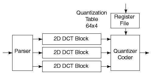
According to the JPEG standard [Wallace] quantization of coefficients is by dividing each of the coefficients in the 8x8 DCT coefficient block by a corresponding value in an 8x8 quantization table, to reduce the bit allocation. In the hardware implementation, this is simply achieved by the quantization table detailing the number of bits to represent each coefficient, and then the coefficient is right shifted appropriately to reduce it to that many bits. The largest possible resulting DCT coefficient is 65280 (256x255), requiring sixteen bits to represent the magnitude, and an additional sign bit as coefficients may be positive or negative [Keating].
The DCT algorithm implemented requires 22 multiplies and 30 additions
for each one-dimensional 8 point DCT [Richardson and Riley] and row-column
decomposition is used to compute the two dimensional DCT. This is pipelined,
so that each three stage pipeline multiplier is in constant use while processing
the image. A diagram of the implementation is shown below (click on it,
to magnify). The multipliers are 16 bit, required for accuracy (eight bit
integer with four bit fractional part, the input values at each stage are
multiplied by one of seven different constants, which range between 0.19
and 0.98 and are represented to 16 binary places).
The stream of data coming in (assumed to be 8x8 24 bit RGB image blocks)
is broken up into each eight bit color component, which goes through the
above pipeline. The final 8x8 DCT coefficients are quantized and output.
This is shown below.
The inverse two dimensional DCT uses the same pipeline, just requiring right shifting of the input 8x8 block of coefficients and the output values, to perform the inverse DCT (this can be done as the 1D DCT and inverse 1D DCT differ in the scaling factor of the DC coefficient and a factor of 16 [Lim]).
Power estimates are accurate to within about a factor of two, while the
speed and area estimates are accurate to within about 20%.
Since the register files between the 1D DCT calculations are "double-buffered",
we can assume that the JPEG encoding is pipelined at the level of a 1D
DCT. Likewise, if we assume that the control logic for the 1D DCT
is intelligent enough not to overwrite values from the previous operation
(add/mult/add), then we can assume that the DCT is "pipelined" for each
operation. Furthermore, if we assume that the multiplier is the critical
resource in the pipeline, then the number of multiplications determine
the "cycle-time" of this pipeline. Lastly, the multiplier itself
is pipelined with a depth of 3 and operates at 25 MHz. From these
assumptions, we can calculate the total encode/decode time as follows:
| Cycle Time | Pipeline Depth | Iterations | Total time | |
| Multiply | 40 ns | 3 | 22 (multiplies per 1D DCT) | 960 ns |
| 1D DCT | 960 ns | 3 | 8 (1D DCT's per block) | 9600 ns |
| Block Processing | 9600 ns | 2 | 4800 (blocks per frame) | 0.046 s |
Note that the total time is the cycle time multiplied with the number of
iterations plus the pipeline depth minus one. Note also that
we have ignored the parser and quantizer/coder blocks, because we have
assumed that they add a few cycles to the latency of the outer-most pipeline.
This corresponds to less than a micro-second and is insignificant.
Based on this number, the power estimates for the register files (which are based on arrays of D-flip-flops) are calculated as twice the switching energy for one word times 25 MHz. Power estimates for the other logic are based on a function of the number of state flip-flops assumed for each functional block. It was assumed that 9 state flip-flops would be needed for the 2D DCT control block, along with 20 flip-flops for the Parser and Quantizer/Coder. From here, the total power was estimated as six times the switching energy of the flip-flops times 25 MHz.
The table below tabulates the power numbers for each block and the chip as a whole. We can calculate the total energy per frame as the total power times the calculation time, 22.2 uJ.
Since gated clocks are used, the static power is limited to the input clock loading, which is assumed to be 25 MHz times the switching energy for 10 D-flip-flops. This gives a static power of 5.3 uW.
The area for the 2D-DCT block was assumed to be twice the sum of the
areas of the sub-blocks (to account for routing area). Likewise,
the area for the entire chip was assumed to be twice the sum of the 2D-DCT
and other blocks' areas.
| Block | Sub-block | ||||
| 2D-DCT Block | words | bits | area (mm2) | power (uW) | |
| Register Files | 64 | 8 | 0.18 | 8.5 | |
| 64 | 8 | 0.18 | 8.5 | ||
| 16 | 11 | 0.068 | 11.7 | ||
| 22 | 16 | 0.12 | 17 | ||
| 64 | 12 | 0.25 | 12.8 | ||
| 64 | 12 | 0.25 | 12.8 | ||
| 16 | 15 | 0.088 | 16 | ||
| 22 | 16 | 0.12 | 17 | ||
| 64 | 16 | 0.32 | 17 | ||
| 64 | 16 | 0.32 | 17 | ||
| area per mult. (mm2) | energy per mult. (pJ) | ||||
| Multipliers | 0.075 | 16 | 0.155 | 80 | |
| area per f-f (mm2) | energy per f-f (pJ) | ||||
| Control Logic | 0.000216 | 0.0213 | 0.0117 | 28.7 | |
| block area: | 4.15 | ||||
| Rest of Chip | words | bits | |||
| Register File | 64 | 4 | 0.113 | 4.25 | |
| area per f-f (mm2) | energy per f-f (pJ) | ||||
| Parser & Quant./Coder | 0.000216 | 0.0213 | 0.00432 | 63.8 | |
| Total for Chip: | 24.9 (mm2) | 483 (uW) |