|
Like Lab 5, this is a long lab! MAKE SURE TO
START EARLY!
Homework Policy: Homework assignments are due in class. No late homeworks will be accepted. There will be a short quiz in lecture the day the assignment is due; the quiz will be based on the homework. Study groups are encouraged, but what you turn in must be your own work.
Lab Policy: Labs reports due by midnight via the submit program. No late labs will be accepted.
As decided in class, the penalty for cheating
on homework or labs is no credit for the full assignment.
Homework 6:Please
do the following problems from P&H: 7.8, 7.12, 7.15, 7.17, 7.19, 7.23,
7.28, 7.33, 7.35, 8.8, 8.12, 8.19, 8.29
Homework assignments should continue to be done
individually.
Lab 6:
In this lab, you will be designing a memory system for your pipelined processor. The previous memory module was far from practical, and you will never have separate, dedicated DRAM banks for instructions and data. Using a realistic main memory system will cause two problems in your pipelined processor: (1) your cycle time will dramatically increase as a result of the main memory write and read latency and (2) you must handle conflicts when both data and instruction accesses occur in the same clock cycle. As you most likely have learned in lecture and in the book, the solution to these problems is the addition of cache memory.
There are some extra-credit options at the end of the lab. If you choose to try these extra-credit options, they may significantly affect your cache architecture. So, make sure to read through the whole lab first. If you choose to build the extra credit options, you are not required to demonstrate a working version with the base parameters. For instance, if you choose to build a fully-associative cache, you are not required to build a 2-way set-associative cache as well.
THIS LAB CAN BE EXTREMELY DIFFICULT, SO AN EARLY START WOULD BE A VERY
GOOD IDEA.
As before, you will be evaluating you and your team members' performance on the last lab assignment (Lab #5). Remember that points are not earned only by doing work, but by how well you work in a team. So if one person does all the work, that certainly does not mean he/she should get all the points!
To evaluate yourself, give us a list of the portions of Lab 5 that you were originally assigned to work on, as well as the set of things that you eventually ended up doing (these are not necessarily the same, and we realize this).
You may give a total of 20 points per person in the group (besides yourself), but do not give any more than 30 points to one person. Submit your evaluations to your TA by email as soon as possible. Make sure to include a one or two line justification of your evaluation.
Email the result to your TA by Wednesday 11/7 at Midnight.
NOTE: Read these instructions carefully. They contain all the information you will need to write your report for this lab, including some requirements not directly related to the cache and memory additions!
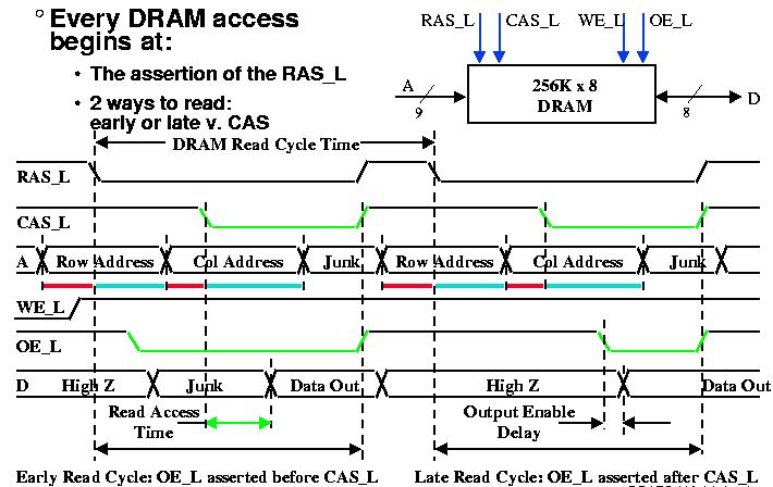
The first step in creating a new memory system is changing the model for our main memory bank (hereafter called the DRAM). The new DRAM, called dram_4k in the U:\cs152\lib library, is slightly simplified version of the DRAM that we discussed in class. It has a 32-bit data bus, with 1024 words in it. Just as in class, there are four control signals, RAS_L, CAS_L, OE_L, and WE_L which control the behavior of the RAM. In addition, there is a "SLOW_H" parameter that will be used to control the speed of the DRAM -- more on this later.
For this problem, design a DRAM controller which has the following entity specification:
entity memory_control isThe processor part of this interface is very simple. When the "request" line is asserted on a falling edge, it is assumed that the "address" and "r_w" signals are stable. In addition, if the "r_w" signal is asserted (equal to "1"), it is then assumed that a write will happen, and the "data_in" signal is stable as well. Immediately afterwards, the "wait" output will be asserted for every cycle until the final cycle of the access (accesses will take more than one cycle). If a read is requested, then you should arrange so that the read data is ready (on the "data_out" bus) on the same clock edge that "wait" is deasserted.
port (
-- Interface to the pipeline
signal clk : in vlbit;
signal request: in vlbit; -- This signal is set to 1 when processor making request
signal r_w : in vlbit; -- This signal is set to 1 if processor doing a write
signal data_in : in vlbit_1d(31 downto 0);
signal data_out : out vlbit_1d(31 downto 0);
signal address : in vlbit_1d(9 downto 0);
signal wait : out vlbit;-- Interface to the DRAM module
signal data_inout : inout vlbit_1d(31 downto 0);
signal addr_out : out vlbit_1d(4 downto 0);
signal RAS_L : out vlbit;
signal CAS_L : out vlbit;
signal OE_L : out vlbit;
signal WE_L : out vlbit;
signal REFRESH_L : out vlbit;-- DRAM speed select signal
signal SLOW_H: in vlbit);
end ram_interfacer;
After the final cycle (falling edge with "wait" deasserted), the processor must set "request" to low or risk starting another access (you have several timing options here -- choose them carefully). One possible timing for a processor read is shown here:
|
Keep in mind that this memory module is word addressed (i.e. the DRAM data bus produces a complete 32-bit word). Don't forget to adjust your processor addresses accordingly (i.e. processor addresses are byte-oriented).
Now, consider the interface to the DRAM. While the processor interface has a 10 bit address, the DRAM interface has only a 5 bit address. This is because the DRAM takes its address in two pieces: the ROW address (which is the top 5 bits) and the COLUMN address (which is the bottom 5 bits). The four DRAM control signals, RAS_L, CAS_L, OE_L, and WE_L must be manipulated in order to properly control the DRAM. In addition, the REFRESH_L signal should be wired to "1" (this turns off refreshing for now -- see the extra credit). Finally, the SLOW_H signal should be externally selectable between "0" (fast) and "1" (slow).
We will be talking more about DRAMs in class, but the key timing diagrams are shown in the following figures:
|
|
|
|
|
|
|
|
You will be designing a RAM controller that is able to handle 2 speeds of DRAM (so called "FAST" and "SLOW"). The following timing parameters must be met for the DRAM:
Given the above timing, the minimum number of edges for a DRAM access becomes three: One for the RAS address, one for the CAS address, and one for the RAS recovery. You don't need to hold up your processor during the RAS precharge cycle (look at the processor read timing diagram: this is the cycle after wait has been deasserted). If your clock cycle time is too short (as it would be if you optimized your processor well), then you need to use more cycles than the minimum. Further, since you probably won't know exactly how long your clock will be (or may be varying it during debugging), you may want to figure out how to lengthen the number of cycles for events automatically when the clock is too short. (Hint-- look at the time between sucessive clock edges and add additional cycles until you have met each spec). Note also that your controller must be able to handle both "FAST" and "SLOW" DRAMs.
It is important to note that the DRAM databus is bidirectional. Thus, if you are writing to the DRAM, data should be driven on the data bus. If you are reading, the data bus should be left in a high-impedance state (this can be accomplished by assigning the bus a "ZZZZZZZZ\h" value).
When writing up this part of the problem, make sure to include timing
diagrams for your processor interface (read and write), as well as your
DRAM interface (read and write). Describe the state-machine that
you used to control your DRAM and include the code for your controller.
Explain
your methodology for testing of the DRAM.
As mentioned for lab 5, we are standardizing delays for components.
Here are the delays that we posted. You should make sure to use them.
| COMPONENT | DELAY |
|
ALU (32-bit):
|
15 ns |
|
VARIABLE ADDER (32-bit):
|
12 ns |
|
FIXED ADDER (32-bit):
|
8 ns |
|
VARIABLE SHIFTER (32-bit):
|
10 ns |
|
CONTROLLER (main and cache):
|
6 ns |
|
COMPARATOR (32-bit):
|
10 ns |
|
Tristate Buffers:
|
|
|
Extender:
|
|
|
Registers:
|
|
|
Register File:
|
|
|
Muxes (2 inputs):
|
|
|
Muxes (3,4 inputs):
|
|
|
Muxes (5+ inputs):
|
|
NOTE: When symbols are made with the VHDL2SYM command or the Symbol Wizard in Workview, the delay values for the components are attached as atttributes to the symbol. You may need to adjust (or simply remove) this value on the symbol even if changes are made to the VHDL entity.
We would like to strongly suggest a heirarchical approach to the design of your cache. This means that you should try to group together subsystems of your cache and create symbols for those subsystems, so that the top level is not too overwhelming. For instance, you may want to combine the data, tag, and status bit(s) into a single symbol that represents all the information associated with each block. You can then tie each of these symbols together to form your cache. Or you may want to combine all data blocks into a single symbol that has an address line coming into it and some information coming out. The reasons for this are that you don't have to waste tons of time tracking down net names and finding broken connections in one large schematic, and it allows you test your design in stages rather than in one big, difficult chunk. The exact structure is entirely up to you, but a clever setup will save both you and your TA a lot of time.
Once your cache is designed, you may test it in one of two ways. The first way: leave your cache as a separate component and test it using vectors and manually assigned signals. If you use this method, you must be careful to keep the testing readable and concise for grading. Remember, we don't like looking at waveforms in the lab report. The second way: you can hook up a new DRAM controller and DRAM TO EACH CACHE and begin testing your design. You do not need to worry about simultaneous requests in this problem, which is why we allow a memory block for each cache. If you are implementing interleaved main memory as extra credit, you are allowed to attach two memory block for each cache. At this point (regardless of which testing method you use), you should begin to evaluate how the addition of cache affected your critical path (since it is required in the report!).
Problem 3: Adding a Single DRAM and Arbitration to Your Processor
After you have your cache ready to go, there is one more problem that
needs to be fixed. Both the data and instruction caches could quite possibly
need to access the DRAM at the same time. You will need to design an arbitration
method for handling simultaneous DRAM requests. Depending on your
cache timing and and how efficient you try to be, this can be the most
difficult and trickiest part of this lab. There is no recommended way to
accomplish this task, but you are certainly allowed to design a single
state machine in VHDL and use it as a memory arbiter/controller; you are
also allowed to modify your DRAM controller from Problem 1. Try to be as
realistic as possible with the delay through this module, and keep in mind
the speed it should have compared to the other components listed above.
Your lab report should contain a description of (a) how your DRAM controller operates, (b) how your cache operates, (c) how you handle DRAM request arbitration, (d) how the addition of your cache amd main memory affected your critical path, and (e) how you determined your component delay values. Make sure to describe your testing methodology: how did your verify that your components worked properly?? In addition, you should include legible schematics, all VHDL code, all diagnostic programs (in assembly language), and Digital Fusion simulation logs (using a good diagnostic and the dumpm command -- no waveforms). If you do the extra credit below, also include a description of how the additional improvements affect your performance and critical path with respect to the minimum requirements.
Extra Credit: Optimizing and Improving Your Cache
Instead of following the bare requirements listed above, you may complete any number of the following problems for extra credit. This means that you do not need to design the basic cache structure above, and then proceed to do the extra credit. You should now consider yourself warned that most of these cannot be easily added onto the requirements above; they are typically entirely different cache architectures. These improvements are not trivial, and may impact your ability to finish the lab on time. ONLY WORKING PROJECTS CAN RECEIVE FULL OR EXTRA CREDIT.

This is called "fast page mode". As you might imagine, you can only access successive words with this mechanism (since you are not changing the ROW address). So, update your memory controller to handle the two words from (or to) the cache at a time, by grabbing two consecutive words from memory. How to actually implement this feature is part of the problem, but you could get almost the same throughput increase as increasing the Memory Bus to 64 bitts(and take as much advantage of the block width of your cache) while only using one DRAM component!
To refresh a row, assert a ROW address, then let RAS_L go low. Make sure that you wait the minimum RAS cycle time before the next falling edge of RAS_L (100ns). Also, make sure that you have the minimum RAS precharge time (50ns). This probably means that a minimum time is 2 cycles -- one to set RAS low, one to set it high.
The key to implementing this feature, is that you need: